- Home/
- GATE ELECTRONICS/
- GATE EC/
- Article
JFET [Junction Field Effect Transistor]
By BYJU'S Exam Prep
Updated on: September 25th, 2023

A JFET is a three-terminal device in which the voltage is applied at one terminal to control the output current. The conduction current is by one type of carrier, either by electrons or by holes. Only the majority of charge carriers are responsible for the current flow. Therefore, JFET is unidirectional.
In this article, you will get an overview of what is a Field effect transistor(FET) and its brief description, and its type, which is JFET. You will learn about the detailed description of JFET’s construction, its types which are N-type and P-type, its modes of operation, its VI characteristics curve, its applications, and some relative advantages and disadvantages.
Download Formulas for GATE Electronics & Communication Engineering – Control System
Table of content
What is a Field Effect Transistor?
The field-effect transistor (FET) is a transistor that uses an electric field to control the current flow. These are devices with three terminals: source, gate, and drain. The current flow can be controlled by applying a voltage to the gate, which alters the conductivity between the drain and the source.
They are also known as unipolar transistors as they involve single carrier type operation, which means they use either electrons or holes as charge carriers in their operation, but not both. There are two types of FETs, one is Junction Field-Effect Transistor (JFET), and the other is a “Metal-Oxide-Semiconductor” Field-Effect Transistor (MOSFET), or Insulated-Gate Field-Effect Transistor (IGFET).
Download Formulas for GATE Electronics & Communication Engineering – Digital Circuits
What is JFET?
JFET is a unidirectional electrical circuit. A JFET is essentially a voltage-driven device. A junction field effect transistor is a three-terminal circuit with an output current controlled by applying a voltage to one terminal.
JFET Full Form
The full form of JFET is Junction Field-Effect Transistor. A JFET is also called a transistor.
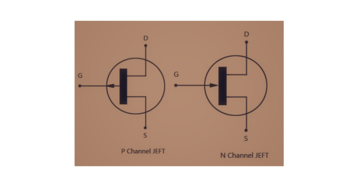
JFET Symbol
The symbol of JFET is shown in the image provided below:
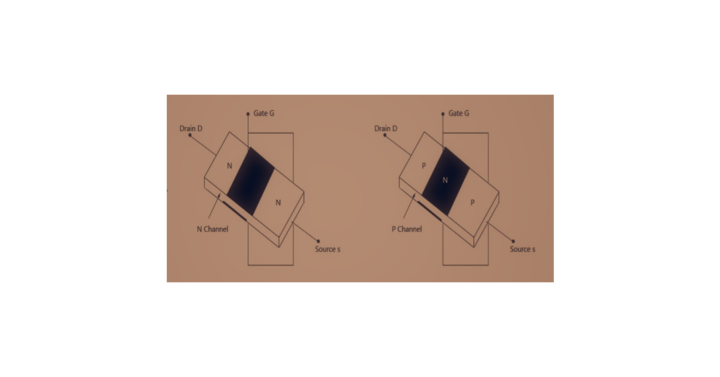
Construction of JFET
In an N-channel JFET, the body is of P-type, and the substrate is N-type; it is doped with donor impurities meaning that the flow of current through the channel is negative in the form of electrons; on the other hand, in P-channel JFET, the body is of N-type and the substrate used is p-type, it is doped with acceptor impurities meaning that the flow of current through the channel is positive in the form of holes.
Download Formulas for GATE Electronics & Communication Engineering – Electronic Devices
Operation of JFET
When no voltage is applied across the source and gate, the channel is like an open path for the carriers to flow through it. When a reverse bias is applied, the channel narrows by increasing the depletion layer and puts the JFET in the cut-off or pinch-off region.
When zero Gate voltage is applied, and a small voltage is applied between the Drain and the Source, maximum saturation current (IDSS) will flow through the channel and be restricted by the small depletion region around the junctions.
When a small negative voltage is applied to the Gate, the size of the depletion region increases, reducing the overall effective area of the channel, and so the current flowing through the channel decreases. When a reverse bias voltage is applied, there is an increase in the width of the depletion region, due to which conduction current reduces through the channel.
When the PN-junction is reverse biased, little current flows into the gate connection. When the Gate voltage is made more negative, channel width decreases until no more current flows through it, and the FET is said to be “pinched-off.” The voltage at which the channel almost closes is called the “pinch-off voltage.”
JFET Characteristics
The VI characteristic curve of P-type and N-type Junction field effect transistors is shown below:
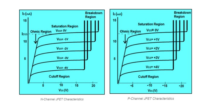
The voltage VGS represents the voltage between the gate and the source, and the voltage VDS represents the voltage between the drain and the source.
The JFET has different stages of operation depending on the input voltages, and the characteristics of JFET in different regions are explained below. It operates in ohmic, saturation, cut-off, and break-down regions.
- Ohmic Region: If the voltage across Gate and Source is zero, then the depletion region of the channel is tiny, and in this region, it acts as a voltage-controlled resistor.
- Pinched-off Region: It is the cut-off region. JFET enters this region when the gate voltage is negative; then, the channel closes; hence no current flows through the channel.
- Saturation or Active Region: In this region, the channel acts as a good conductor, which is controlled by the gate voltage.
- Breakdown Region: If the drain to source voltage is very high, then the channel of the JFET breaks down, and uncontrolled maximum current passes through the device.
Applications of JFET
JFET has a high impedance. These are low power consumption devices, and they are smaller in size, have more gate current, and have low modulation distortion, so with regards to these advantages, there are many applications of JFET. Some applications of JFET are given below:-
- JFET is used as a switch, JFET amplifier, and buffer.
- JFET is used as a chopper.
- JFET is used in oscillatory circuits because of its low frequency, used in cascade amplifiers in RF amplifiers.
- Used in digital circuits because of their small size.
- Used in communication equipment because of their low modulation distortion.
- Used as voltage-controlled resistors in operational amplifiers.
|
Important GATE Topics |
|
| Portal Frames | Superposition Theorem |
| Binary Search Tree | Work Done By A Constant Force |
| Structural Analysis | Motion Under Gravity |
| Basic Signal Operations | Ideal Diode |