Time Left - 01:00:00 mins
GATE EC : Electronic Devices & Circuits - National Champion Test
Attempt now to get your rank among 651 students!
Question 1
An n-type silicon sample is uniformly illuminated with light which generates 1020 electron hole pairs per cm3 second. The minority carrier lifetime in the sample is 1 μs. In the steady state, the hole concentration in the sample is approximately 10x, where x is an integer. The value of x is___
Question 2
Which of the following option will provide the least resistance across the bulb?
Question 3
Two resistance R1 and R2 give combined resistance of 4.5 ohms when in series and 1 ohm when in parallel. The resistance are
Question 4
Thin gate oxide in a CMOS process in preferably grown using
Question 5
What is the output waveform V0 for a sinusoidal input of peak-peak amplitude of 4V. Assume that Z1 and Z2 are two identical Zener diodes of 4.7V, and R1=10kohm and R2=20kohm.

Question 6
How could Schrodinger’s equation be relevant in the practical design of a Cathode- Ray Tube?
Question 7
The power rating of a 470 ohm resistor carrying a current of 40mA should be
Question 8
In the circuit shown, assume that diodes D1 and D2 are ideal. In the steady state condition, the average voltage Vab (in Volts) across the 0.5 μF capacitor is _______.

Question 9
For a particular toroidal inductor core, the inductance value obtained for 50 Turns is 200μH. If two such inductors are wired in parallel, the resulting inductance is
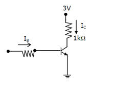
Question 10
Assuming VCEsat = 0.2 V and β = 50, the minimum base current (IB) required to drive the transistor in figure to saturation is?
Question 11
In the circuit shown below, the Zener diode is ideal and the Zener voltage is 6V. The output voltage V0 (in volts) is ____________.

Question 12
An n-type silicon bar 0.1 cm long and µm3 in the cross-sectional area has a majority carrier concentration of 5 × 10²⁰/m3 and the carrier mobility is 0.13 m2/V–s at 300 K. If the charge of an electron is 1.6 × 10⁻¹⁹ coulomb, if the area of the bar is (Area = 100 * 10-12) then the resistance of the bar is
Question 13
The silicon sample with unit cross-sectional area shown below is in thermal equilibrium. The following information is given: T = 300K, electronic charge =1.6 × 10⁻¹⁹C, thermal voltage = 26mV and electron mobility = 1350cm2/V–s

The magnitude of the electric field at x = 0.5 μm is
The magnitude of the electric field at x = 0.5 μm is
Question 14
If C denotes the counterclockwise unit circle, the value of the contour integral  is ______
is ______Question 15
The action of a JFET in its equivalent circuit can best be represented as a
Question 16
What is the output voltage across the 900 ohm load in the circuit given below?

Question 17
Which one of the following is the lowest level of abstraction for representation of a digital system?
Question 18
A coaxial capacitor of inner radius 1 mm and outer radius 5 mm has a capacitance per unit length of 172 pF/m. If the ratio of outer radius to inner radius is doubled, the capacitance per unit length (in pF/m) is ___.
Question 19
A MOS capacitor made using p type substrate is in the accumulation mode. The dominant charge in the channel is due to the presence of
Question 20
The magnitude of the electron drifts current density at
x = 0.5 μm is
x = 0.5 μm is
Question 21
A square pulse of 3 volts amplitude is applied to C-R circuit shown in figure. The capacitor is initially uncharged. The output voltage v0 at time t = 2 sec is


Question 22
In the circuit shown in the figure, the BJT has a current gain (β) of 50. For an emitter-base voltage VEB = 600 mV, the emitter-collector voltage VEC (in Volts) is _____.

Question 23
If the base width in a bipolar junction transistor is doubled, which one of the following statements will be TURE?
Question 24
The desirable properties of transformer core material are
Question 25
The transistors used in a portion of the TTL gate shown in figure have β =100. The base-emitter voltage of is 0.7V for a transistor in active region and 0.75V for a transistor in saturation. If the sink current I =1mA and the output is at logic 0, then the current IR will be equal to

Question 26
The neutral base width of a bipolar transistor, biased in the active region, is 0.5 μm. the maximum electron concentration and the diffusion constant in the base are 1014/cm3 and Dn = 25 cm2/sec respectively. Assuming negligible recombination I the base, the collector current density is (the electron charge is 1.6 × 10⁻¹⁹ coulomb)
Question 27
In a uniformly doped BJT, assume that NE, NB and NC are the emitter, base and collector dopings in atoms/cm3, respectively. If the emitter injection efficiency of the BJT is close unity, which one of the following conditions is TRUE?
Question 28
For the BJT Q1 in the circuit shown below, β = ∞, VBEon = 0.7 V, VCEsat = 0.7 V. The switch is initially closed. At time t = 0, the switch is opened. The time t at which Q1 leaves the active region is

Question 29
For an npn transistor connected as shown in figure, VBE = 0.7 Volts. Given that reverse saturation current of the junction at room temperature 300 °K is 10-13 A, the emitter current is

Question 30
The source of a silicon (ni = 1010 per cm3) n-channel MOS transistor has an area of 1 sq μm and a depth of 1 μm. If the dopant density in the source is 1019/cm3, the number of holes in the source region with the above volume is approximately
- 651 attempts
- 5 upvotes
- 37 comments
Nov 28ESE & GATE EC

