Time Left - 30:00 mins
ESE EC : Digital Circuits - National Champion Test
Attempt now to get your rank among 336 students!
Question 1
In order to build a 3 bit simultaneous A/D converter, what is the number of comparator circuits required?
Question 2
A 10-bit A/D converter is used to digitize an analog signal in the 0 to 5 V range. What is the approximate value of the maximum peak to peak ripple voltage that can be allowed in the d.c. supply voltage?
Question 3
In which one of the following types of analog to digital converters the conversion time is practically independent of the amplitude of the analog signal?
Question 4
Which of the following A/D converter is used in a Digital Storage Oscilloscope (DSO)?
Question 5
What is the output voltage ‘V0’ of the R-2R decoder ladder network?

Question 6
Two 2’s complement numbers having sign bits ‘x’ and ‘y’ and added and the sign bit of the result is ‘z’. Which Boolean function indicates the occurrence of the overflow?
Question 7
The Boolean functions can be expressed in canonical SOP (sum of products) and POS (product of sums) form. For the functions  , which are such two forms
Question 8
In NOR-NOR configuration. The minimum number NOR gates needed to implement the switching function
![]() is.
is.
Question 9
The difference between PLA and ROM is.
Question 10
Which one of the following statements is correct?
Question 11
A Gray code is a/an:
Question 12
If (2.3)base4 + (1.2)base4 = (y)base4; what is the value of y?
Question 13
Match List-I (Type of flip-flop) with List-II (Symbol) and select the correct answer using the code given below the lists:
List- I
A). T flip-flop
B). Level-triggered JK flip-flop
C). Leading edge-triggered JK flip-flop
D). Trailing edge-triggered JK flip-flop
List- II
1).
2).
3).
4).
List- I
A). T flip-flop
B). Level-triggered JK flip-flop
C). Leading edge-triggered JK flip-flop
D). Trailing edge-triggered JK flip-flop
List- II
1).
2).
3).
4).
Question 14
Consider the following statements:
For a master-slave J-K flip-flop.
1). the toggle frequency is the maximum clock frequency at which the flip-flop will toggle reliably.
2). the data input must precede the clock triggering edge transition time by some minimum time.
3). the data input must remain fixed for a given time after the clock triggering edge transition time for reliable operation.
4). Propagation delay time is equal to the rise time and fall time of the data.
Which of the above statements is/are correct?
Question 15
In the circuit given below, both transistors have the same VT. What is the approximate value of the highest possible output voltage  , if Vin can range from 0 to VDD? (Assume
 ).
).

Question 16
Consider the following statements describing the property of a complementary MOS (CMOS) inverter:
1). It is a combination of an n-channel FET and a p-channel FET.
2). There is power dissipation when the input carries the logical 1 signal.
3). There is no power dissipation when the input carries the logical 1 signal.
4). There is power dissipation during transition from 0 to 1 or from 1 to 0
Which of the statements given above are correct?
Question 17
Which of the following statements in not correct?
Question 18
Assertion (A): The speed-power product is an important parameter for comparing various TTL series.
Reason (R): A low value of speed-power product indicates that a propagation delay can be achieved without excessive power dissipation and vice-versa.
Reason (R): A low value of speed-power product indicates that a propagation delay can be achieved without excessive power dissipation and vice-versa.
Question 19
Which of the following output configurations are available in a TTL gate?
1). Open collector output
2). Totem-pole output
3). Tristate output
Select the correct answer from the codes given below:
1). Open collector output
2). Totem-pole output
3). Tristate output
Select the correct answer from the codes given below:
Question 20
Statements (I): Switching speed of ECL logic family is very high
Statements (II): The transistor used in the family remains unsaturated..
Statements (II): The transistor used in the family remains unsaturated..
Question 21
The Boolean expression for the output of the below logic circuit is.
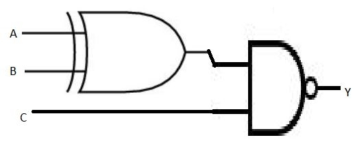
Question 22
Assume that only x and y logic inputs are available, and their complements  and
and  are not available. What is the minimum number of 2-input NAND gates required to implement x⊕y?
Question 23
The Boolean expression  is to be realized using only two 2-input gates. Which are these gates?
- 336 attempts
- 3 upvotes
- 10 comments
Jun 9ESE & GATE EC

