Time Left - 01:00:00 mins
GATE EC : Digital Circuits - National Champion Test
Attempt now to get your rank among 760 students!
Question 1
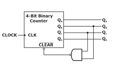
A mod-n counter using a synchronous binary up–counter with synchronous clear input is shown in the figure. The value of n is__________
Question 2
A 4-bit presetable asynchronous UP counter has preset state output 0101. The preset operation takes place as soon as the counter reaches 1111. The modulus of the counter is
Question 3
Principle of "locality" is used in context of
Question 4
"Cycle Stealing" in microprocessor parlance refers to
Question 5
When L is doubled and C is halved, the resonance frequency of series tuned circuit becomes
Question 6
How many 1’s are present in the binary representation of 3 x 512 + 7 x 64 +5 x 8 + 3 ?
Question 7
The output Y of a 2-bit comparator is logic 1 whenever the 2-bit input A is greater than the 2-bit input B. The number of combinations for which the output is logic 1, is
Question 8
In the circuit shown diodes D1, D2 and D3 are ideal, an the inputs E1, E2 and E3 are “0 V” for logic ‘0’ and “10 V” for logic ‘1’. What logic gate does the circuit represent?

Question 9
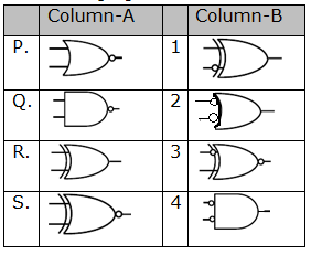
Match the logic gates in Column A with their equivalents in Column B.
Question 10
Figure shows the internal schematic of a TTL AND-OR-Invert (AOI) gate. For the inputs shown in Figure, the output Y is

Question 11
Consider a binary digital communication system with equally likely 0’s and 1’s. When binary 0 is transmitted the voltage at the detector input can lie between the level s-0.25V and +0.25V with equal probability: when binary 1 is transmitted, the voltage at the detector can have any value between 0 and 1 V with equal probability. If the detector has a threshold of 2.0V (i.e., if the received signal is greater than 0.2 V, the bit is taken as 1), the average bit error probability is
Question 12
The minimum number of 2 to 1 multiplexers required to realize a 4 to 1 multiplexer is
Question 13
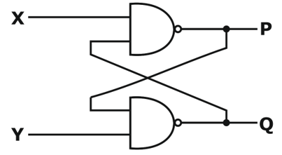
The following binary values were applied to the X and Y inputs of the NAND latch shown in the figure in the sequence indicated below:
X = 0, Y = 1;
X = 0, Y = 0;
X = 1, Y = 1
The corresponding stable P, Q outputs will be:
X = 0, Y = 1;
X = 0, Y = 0;
X = 1, Y = 1
The corresponding stable P, Q outputs will be:
Question 14
Assuming that flip-flops are in reset condition initially, the count sequence observed at QA in the circuit shown is

Question 15
What memory address range is NOT represented by chip #1 and chip #2 in figure? A0 to A15 in this figure are the address lines and CS means Chip Select. Which one of the following is not performed by this sequence?

Question 16
In the circuit shown in figure, A is a parallel in, parallel–out 4–bit register, which loads at the rising edge of the clock C. The input lines are connected to a 4–bit bus, W. Its output acts as the input to a 16 × 4 ROM whose output is floating when the enable input E is 0. A partial table of the contents of the ROM is as follows :


The clock to the register is shown, and the data on the W bus at time t1 is 0110. The data on the bus at time t2 is
The clock to the register is shown, and the data on the W bus at time t1 is 0110. The data on the bus at time t2 is
Question 17
Silicon is doped with boron to a concentration of 4×10¹⁷ atoms/cm3. Assuming the intrinsic carrier concentration of silicon to be 1.5×10¹⁰/cm3 and the value of ![]() to be 25 mV at 300 K
to be 25 mV at 300 K
Compared to undoped silicon, the Fermi level of doped silicon?
Question 18
An I/O peripheral device shown in figure (b) below is to be interfaced to an 8085 microprocessor. To select the I/O device in the I/O address range D4 H – D7 H, its chip-select  should be connected to the output of the decoder shown in figure (a) below:

Question 19
The content (in Hexadecimal) of some of the memory locations in an 8085A based system are given below:

The contents of stack pointer (SP), program counter (PC) and (H,L) are 2700H, 2100H and 0000H respectively. When the following sequence of instructions are executed,
2100 H: DAD SP
2101 H: PCHL
the contents of (SP) and (PC) at the end of execution will be
The contents of stack pointer (SP), program counter (PC) and (H,L) are 2700H, 2100H and 0000H respectively. When the following sequence of instructions are executed,
2100 H: DAD SP
2101 H: PCHL
the contents of (SP) and (PC) at the end of execution will be
Question 20
An 8085 executes the following instructions
2710 LXI H, 30A0H
2713 DAD H
2714 PCHL
All addresses and constants are in Hex. Let PC be the contents of the program counter and HL be the contents of the HL register pair just after executing PCHL. Which of the following statements is correct?
2710 LXI H, 30A0H
2713 DAD H
2714 PCHL
All addresses and constants are in Hex. Let PC be the contents of the program counter and HL be the contents of the HL register pair just after executing PCHL. Which of the following statements is correct?
Question 21
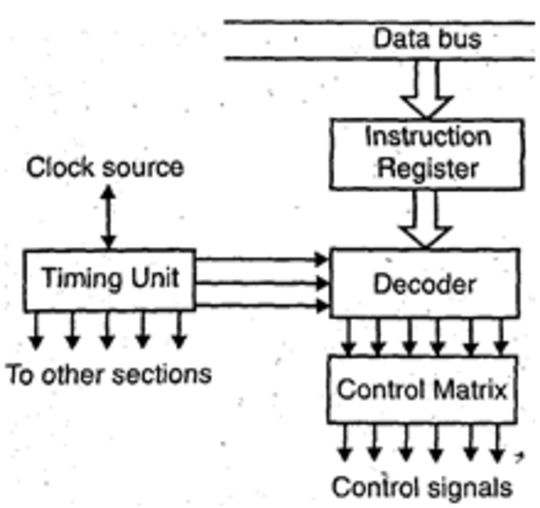
In timing and control circuit of 8085, synchronization is required for
Question 22
A portion of the main program to call a subroutine SUB in an 8085 environment is given below.
:
:
LXI D,DISP
LP : CALL SUB
:
It is desired that control be returned to LP+DISP+3 when the RET instruction is executed in the subroutine. The set of instructions that precede the RET instruction in the subroutine are
:
:
LXI D,DISP
LP : CALL SUB
:
It is desired that control be returned to LP+DISP+3 when the RET instruction is executed in the subroutine. The set of instructions that precede the RET instruction in the subroutine are
Question 23
It is desired to multiply the numbers 0AH by 0BH and store the result in the accumulator. The numbers are available in registers B and C respectively. A part of the 8085 program for this purpose is given below:
MVI A, 00H
Loop; - - - - - - - - - -
…………………………..
…………………………..
HLT END
The sequence of instruction to the complete the program would be
MVI A, 00H
Loop; - - - - - - - - - -
…………………………..
…………………………..
HLT END
The sequence of instruction to the complete the program would be
Question 24
Consider the sequence of 8085 instructions given below.
LXI H, 9258
MOV A, M
CMA
MOV M, A
Which one of the following is performed by this sequence?
LXI H, 9258
MOV A, M
CMA
MOV M, A
Which one of the following is performed by this sequence?
Question 25
All the logic gates shown in the figure have a propagation delay of 20 ns. Let A = C = 0 and B = 1 until time t = 0. At t = 0, all the inputs flip (i.e., A = C = 1 and B = 0) and remain in that state. For t > 0, output Z = 1 for a duration (in ns) of _________.

Question 26
The point P in the following figure is stuck-at-1. The output f will be

Question 27
In the modulo-6 ripple counter shown in Figure, the output of the 2-input gate is used to clear the J-K flip-flops.

The 2-input gate is:
The 2-input gate is:
Question 28
A one-bit full adder is to be implemented using 8-to-1 multiplexers (MUX).
Write the truth table for sum (S) and carry to the next stage (CN) in terms of the two bits (A, B) and carry from the previous stage (C p). The truth table should be in the ascending order of (A, B, Cp), i.e. (000, 001, 010, … etc.).
Write the truth table for sum (S) and carry to the next stage (CN) in terms of the two bits (A, B) and carry from the previous stage (C p). The truth table should be in the ascending order of (A, B, Cp), i.e. (000, 001, 010, … etc.).
Question 29
Implement S and CN using 8-to-1 multiplexers.
Question 30
The figure shows a binary counter with synchronous clear input. With the decoding log shown, the counter works as a

- 760 attempts
- 7 upvotes
- 29 comments
Jun 2ESE & GATE EC

