GATE EE : Analog Electronics - National Champion Test
Attempt now to get your rank among 702 students!
Question 1
When a bipolar junction transistor is operating in the saturation mode, which one of the following statements is TRUE about the state of its collector-base (CB) and the base-emitter (BE) junctions?
Question 2
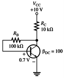
Calculate the Q-point values (IC and VCE) for this circuit ?
Question 3
The common emitter forward current gain of the transistor shown is . The transistor is operating in
Question 4
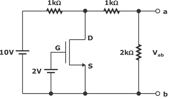
Assume that the N-channel MOSFET shown in the following figure is ideal, and its threshold voltage is +1.0V. The voltage Vab between nodes a and b is:
Question 5
What are the states of the three ideal diodes of the circuit shown in figure?
Question 6
The forward resistance of the diode shown in the following figure is 5 and the remaining parameters are same as those of an ideal diode. The dc component of the source current is
Question 7
The operational amplifier shown in the figure is ideal. The input voltage (in Volt) is . The amplitude of the output voltage V0 (in Volt) is _____.
Question 8
The operational amplifier shown in the figure is ideal. The input voltage (in Volt) is . The amplitude of the output voltage V0 (in Volt) is _____.
Question 9
Which statement is correct in case of ideal OPAMP?
Question 10
An op-amp has an open-loop gain of 105 and an open-loop upper cutoff frequency of 10 Hz. If this op-amp is connected as an amplifier with a closed-loop gain of 100, then the new upper cutoff frequency is
Question 11
The block diagrams of two types of half wave rectifiers are shown in the figure. The transfer characteristics of the rectifiers are also shown within the block. It is desired to make full wave rectifier using above two half-wave rectifiers. The resultant circuit will be
Question 12
In an NMOS circuit, Vt = 4 V and VGS ranges from 7.5 to 10 V. The channel to be continuous, finds the largest value of VDS?
Question 13
A common emitter silicon transistor amplifier with quiescent emitter current as 1mA, what will be the base biasing voltage?
Question 14
The circuit shown in below, is equivalent to a load of
Question 15
In the circuit shown in Figure, the current gain (β) of the ideal transistor is 10. The operating point of the transistor (Vcc, Ic) is
Question 16
For the n–channel enhancement MOSFET shown in Figure below, the threshold voltage Vth= 2 V. The rain current ID of the MOSFET is 4 mA when the drain resistance RD is 1 kΩ. If the value of RD is increased to 4 Ω, drain current ID will become
Question 17
A clipper circuit is shown below. Assume forward voltage drops of the diodes to be 0.7 Volt, the input- output characteristics of the circuit is
Question 18
Which statement is not correct in case of precision half wave rectifier?
Question 19
What is the Maximum Power Efficiency in Class B amplifier circuit
Question 20
A relaxation oscillator is made using oPAMP as shown in figure. The supply voltaged of the OPAMP are ±12V. The voltage waveform at point P will be