Time Left - 12:00 mins
ISRO EC 2019: Analog Circuits Booster Quiz 2
Attempt now to get your rank among 515 students!
Question 1
Consider the following statements related to the flow of current in a PN junction diode:
1. The reverse bias current is due to the diffusion of minority charge carriers.
2. The reverse bias current is due to the drift of thermally generated carriers in the depletion region.
3. The forward bias current is due to the diffusion of minority charge carriers.
4. The forward bias current is due to the drift of majority charge carriers.
Which of the following statement is/are not true?
Question 2
Transformer utilization factor (TUF) for the rectifiers is
Question 3
Consider the junction of a p-n diode. Suppose the p side is now heavily doped with acceptor atoms. Such junction is called as one sided. Consider the following statements now:
The p-n junction has ND =1023m-3 and NA=1026 m-3 and
Built-in potential 1V.
The depletion width is equal to?
Question 4
A BJT is often referred as a bipolar device. It is because:
Question 5
Determine the dc bias voltage  , if
, if  for the given network.

Question 6
Which statement is correct in case of ideal OPAMP?
Question 7
The input resistance  of the circuit in figure is

of the circuit in figure is Question 8
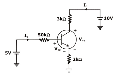
In the circuit shown transistor has β = 100. VBE(sat) = 0.8 V and VCE(sat) = 0.2 V. Then the region of operation
Question 9
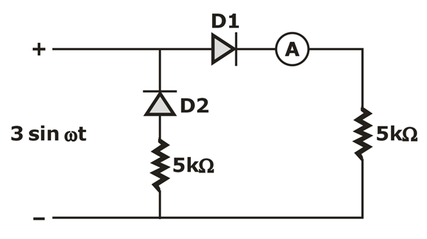
For the circuit given in figure below, find the reading of the ammeter. [assume the diode to be ideal].
Question 10
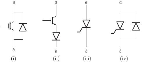
The figure shows four electronic switches (i), (ii), (iii) and (iv). Which of the switches can block voltages of either polarity (applied between terminals 'a' and 'b') when the active device is in the OFF state?
- 515 attempts
- 4 upvotes
- 3 comments
Mar 14ESE & GATE EC

