Time Left - 12:00 mins
ISRO EC 2019: Analog Circuits Booster Quiz 3
Attempt now to get your rank among 549 students!
Question 1
Both transistors T1 and T2 in figure have a threshold voltage of 1 Volt. The device parameters K1 and K2 and T1 and T2 are, respectively, 36 µA/V2 and 9 µA/V2. The output voltage V0 is

Question 2
The diodes and capacitors in the circuit shown are ideal. The voltage v(t) across the diode D1 in steady state is

Question 3
If the differential voltage gain and the common mode voltage gain of a differential amplifier are 48 dB and 2 dB respectively, then its common mode rejection ratio is
Question 4
The amplifier circuit shown below uses a silicon transistor. The capacitors CC and CE can be assumed to be short at signal frequency and the effect of output resistance r0 can be ignored. If CE is disconnected from the circuit, which one of the following statements is TRUE?

Question 5
In the circuit shown, V0 = V0A for switch SW in position A and V0 = V0B for SW in position B. Assume that the opamp is ideal. The value of  is _____________

Question 6
A good current buffer has
Question 7
In a MOSFET operating in the saturation region, the channel length modulation effect causes
Question 8
In a half-wave rectifier, if an a.c supply is 60 Hz. Then what is the a.c ripple at output?
Question 9
A regulated power supply, shown in figure below has an unregulated input (UR) of 15 Volts and generates a regulated output Vout. Use the component values shown in the figure.
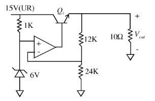
In the figure above, the ground has been shown by the symbol.
In the figure above, the ground has been shown by the symbol.
The power dissipation across the transistor Q1 shown in the figure is:
Question 10
Consider the circuit shown in figure (a), the signal applied as input to the circuit is Vin [shown in figure (b)] 

The voltage across diode VD is given as (Assuming diode to be ideal)
- 549 attempts
- 9 upvotes
- 3 comments
Feb 23ESE & GATE EC

