DAC and ADC: It is possible to convert the analog signal to digital and vice-versa. We can get analog from digital through DAC and can get digital from analog through ADC.
Digital to Analog Converter (DAC): D/A converter (also called a DAC) accepts an n-bit digital word and produces an analog sample.


where, k = Proportionality factor, bn = 1;if nth bit of digital input is 1, bn = 0; if nth bit of digital input is 0.
Classification of DAC:

Weighted Resistor DAC (N – bit):
- A DAC can be constructed by using a Summing Amplifier and a set of resistors R, 2R, 4R, 8R, etc as its inputs.
- The circuit consists of a reference voltage Vf, N binary-weighted resistors R, 2R, 4R, 8R, . . . , 2(N-1) R, N single-pole double-throw switches, and an Op-amp together with its feedback resistance Rf = R/2.
- The switches are controlled by an N-bit digital input word D.
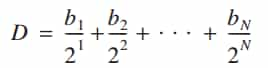

V0 = -Rf If = -Vf D

LSB resistance = (2N – 1) MSB resistance.
- The accuracy of the DAC depends critically on the accuracy of the Reference voltage, the precision of the binary-weighted resistors, and the perfection of the switches.
- A disadvantage of the binary-weighted resistor network is that for a large number of bits (N > 4) the spread between the smallest and largest resistances becomes quite large. This implies difficulties in maintaining accuracy in resistor values.
R – 2R Ladder DAC: Non-Inverting OP-amp type DAC


Inverting Amplifier


Inverted Ladder R – 2R Circuit


![]()

Specifications for DAC:
- Resolution in DAC is changed in analog output with corresponding to 1 LSB bit increment at the input.
- Resolution = weight of LSB =
- V= Voltage corresponding to logic N = Number of bits.
- Analog Output Analog output = resolution x decimal equivalent of binary data
- Maximum Analog Output Voltage (VFS) VFS is the maximum analog output voltage of DAC.
![]()
VFS = Vr
- Percentage Resolution:
![]()
- Maximum Error Maximum error acceptable in ADC and DAC equals to resolution.
- Resolution (R-2R ladder type) =

Analog to Digital Converter:
- A/D converter (also called an ADC) accepts an analog sample VA and produces an N-bit digital word.
- Examples of ADC usage are digital volt meters, cell phone, thermocouples, and a digital oscilloscope.
- Types of A/D Converters: Dual Slope A/D Converter, Successive Approximation A/D Converter, Flash A/D Converter, Delta-Sigma A/D Converter, etc.
Counter type ADC:

- In N-bit counter type ADC:
- Maximum number of clock pulses required for conversion = 2N -1
- Maximum time required for conversion = (2N -1) TCLK
- Minimum number of clock pulses = 1
- Average number of clock pulses = 2N-1
Successive Approximation Type ADC:
- It is faster than digital ramp ADC.
- Conversion time (tc) is independent of the value of the analog input voltage (Va).
- It has fixed conversion time.

- Maximum number of clock pulses = N for conversion
- Maximum conversion time = N.TCLK
Flash Type ADC:
- It is also known as Parallel-comparator type ADC or Simultaneous converter.
- It is highest speed ADC (fastest ADC)
- Functional component
- It utilizes 2N -1 comparators to compare the input signal level with each of the 2N -1 possible quantization levels.
- The outputs of the comparators are processed by an encoding-logic block to provide the N bits of the output digital word.
- Complete conversion can be obtained within one clock cycle.
- For N-bit comparator:
- Total number of comparators = 2N -1,
- Total number of resistors = 2N,
- Total number of priority encoders = 1 (2N × N)
2-bit Flash Converter:

Dual Slope Integrating Type ADC:
- It has slowest conversion time but has relatively low cost.
- The following components are present in the Dual slope A/D converter:
- Integrator
- Electronically Controlled Switches
- Counter
- Clock
- Control Logic
- Comparator


where, n = Count recorded in the counter.
Dual Slope Integrating Type ADC:
- Total number of clock pulses = 2N + n
- Maximum number of clock pulses = 2N + 2N - 1 = 2N + 1 -1== 2N + 1

You can avail of BYJU’S Exam Prep Online classroom program for all AE & JE Exams:
BYJU’S Exam Prep Online Classroom Program for AE & JE Exams (12+ Structured LIVE Courses)
You can avail of BYJU’S Exam Prep Test series specially designed for all AE & JE Exams:
BYJU’S Exam Prep Test Series AE & JE Get Unlimited Access to all (160+ Mock Tests)
Thanks
Team BYJU’S Exam Prep
Download BYJU’S Exam Prep APP, for the best Exam Preparation, Free Mock tests, Live Classes.


Comments
write a comment