1. Integrated Circuits
- Integrated circuits (ICs) are chips, pieces of semiconductor material, that contain all of the transistors, resistors, and capacitors necessary to create a digital circuit or system.
- The first ICs were fabricated using Ge BJTs in 1958.
- Jack Kirby of Texas Instruments, Nobel Prize in 2000
- Robert Noyes of Fairchild Semiconductors fabricated the first Si ICs in 1959.
Integration Levels:
- SSI Small scale integration [12 gates/chip]
- MSI Medium scale integration [100 gates/chip]
- LSI Large scale integration [1K gates/chip]
- VLSI Very large scale integration [10K gates/chip]
- ULSI Ultra large scale integration [100K gates/chip]
Moore's Law:
- A prediction made by Moore (a co-founder of Intel) in 1965: “… a number of transistors to double every 2 years.”
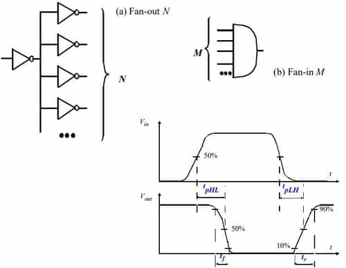
Characteristics of digital circuits
- Fan in:
- Fan in is the number of inputs connected to the gate without any degradation in the voltage level.
- Fan out:
- Fan out specifies the number of standard loads that the output of the gate can drive without impairment of its normal operation
- Power dissipation:
- Power dissipation is a measure of power consumed by the gate when fully driven by all its inputs.
- Propagation delay:
- Propagation delay is the average transition delay time for the signal to propagate from input to output when the signals change in value. It is expressed in ns.
- Noise margin:
- It is the maximum noise voltage added to an input signal of a digital circuit that does not cause an undesirable change in the circuit output. It is expressed in volts.
2. Logic Families
Logic families are sets of chips that may implement different logical functions but use the same type of transistors and voltage levels for logical levels and for the power supplies. These families vary by speed, power consumption, cost, voltage & current levels. The most widely used families are:
- DL (Diode- logic)
- DTL (Diode-transistor logic)
- RTL (Resistor-transistor logic)
- TTL (Transistor -transistor logic)
- ECL (Emitter-coupled logic)
- MOS (Metal-oxide semiconductor)
- CMOS (Complementary Metal-oxide semiconductor)
3. Digital IC Terminology
Voltage Parameters:
- VIH(min): high-level input voltage, the minimum voltage level required for a logic 1 at an input.
- VIL(max): low-level input voltage
- VOH(min): high-level output voltage
- VOL(max): low-level output voltage
- For proper operation, the input voltage levels to a logic must be kept outside the indeterminate range. Lower than VIL(max) and higher than VIH(min).
Noise Margin:
- The maximum noise voltage that can be tolerated by a circuit is termed its noise immunity (noise Margin)

Current Parameters:
- IOH – Current flowing into an output in the logical “1” state under specified load conditions
- IOL – Current flowing into an output in the logical “0” state under specified load conditions
- IIH – Current flowing into an input when a specified HI level is applied to that
input - IIL – Current flowing into an input when a specified LO level is applied to that
input
4. Diode Logic (DL)
- simplest; does not scale
- NOT not possible (need an active element)

5. Resistor-Transistor Logic (RTL)
- replace diode switch with a transistor switch
- can be cascaded
- large power draw

6. Diode-Transistor Logic (DTL)
- essentially diode logic with transistor amplification
- reduced power consumption
- faster than RTL

7. Transistor-transistor logic (TTL)
- based on bipolar transistors one of the most widely used families of small- and medium-scale devices – rarely used for VLSI
- typically operated from a 5V supply
- typical noise immunity about 1 – 1.6 V
- many forms, some optimised for speed, power, etc.
- High-speed versions comparable to CMOS (~ 1.5 ns)
- low-power versions down to about 1 mW/gate
TTL NAND Gate:
- Input terminals: The emitter of Q1
- Output terminals: collector of Q2
- When any input = logic ‘0’
- Q1 emitter junction is forward biased.
- Also, its collector junction is FB,
- so Q1 goes in saturation.
- Base of Q2 is at Low voltage
- This causes base-emitter junction of Q2 to be RB, so Q2 goes in cut-off
- Hence output is 5V or logic ‘1’
- When all inputs = logic ‘1’
- Q1 emitter junction is RB.
- so Q1 goes in cut-off.
- Its collector voltage increases
- This forward biases Q2,
- so Q2 goes into saturation
- Hence output is 0V

A TTL NAND gate with open collector output:
- Its similar to the previous circuit.
- Q2 is used as an emitter follower. The output of Q2 is fed to the input of Q3. Collector of Q2 and Q3 are in phase.
- This circuit needs an external ‘Pull- up’ resistor between output and power supply.
- The disadvantage of open- collector gate is their slow switching speed.
- The pull-up resistance is few kilo ohms. Gives a relatively long time constant, when multiplied by the stray output capacitance.
- Is worst when output goes from low to high.

TTL NAND gate with totem pole (active pull-up):
- In this circuit Q1 and the 4KΩ resistor act like a 2 input AND gate. The remaining circuit acts like an inverter. Transistors Q3 & Q4 form a totem-pole i.e.one NPN transistor in series with another.
- With a totem-pole output stage either Q3 or Q4 is on. When Q3 is ‘on’ output is high. When Q4 is ‘on’ output is low. If A or B is low, the Q1 conducts and the base voltage of Q2 is almost zero.
- Q2 cuts off, hence Q4 goes into cut off. Q3 base is high, Q3 acts as an emitter follower, the output Y’ is high.
- If A and B are high, Q1 does not conduct (cut-off), Q2 base goes high (saturation). Q4 goes into saturation hence output is low.
- The drop across Diode D3 keeps the base emitter diode of Q3 reverse biased. Hence Q3 is off or else it conducts slightly when output is low.
- Now only Q4 conducts when output is low. Totem pole transistors produce a low output impedance. When Q3 is conducting the output impedance is approx 70 Ω. When Q4 is saturated the output impedance is only 12 Ω. Hence the output impedance of a totem pole circuit is low.
- Any stray output capacitance is rapidly charged or discharged through the low output impedance. Hence the output can change quickly from one state to the other.

Types of TTL:
- Standard TTL
- typical gate propagation delay of 10ns and a power dissipation of 10 mW per gate, for a power–delay product (PDP) or switching energy of about 100 pJ
- Low-power TTL (L)
- slow switching speed (33ns)
- reduction in power consumption (1 mW) (now essentially replaced by CMOS logic)
- High-speed TTL (H)
- faster switching than standard TTL (6ns)
- but significantly higher power dissipation (22 mW)
- Schottky TTL (S)
- used Schottky diode clamps at gate inputs to prevent charge storage and improve switching time. A Schottky diode has a very low forward-voltage drop of 0.15–0.45V approx (silicon diode has a voltage drop of 0.6–1.7V). This lower voltage drop can provide higher switching speed.
- Faster speed of (3ns) but had higher power dissipation (19 mW)
- Low-power Schottky TTL (LS)
- used the higher resistance values of low-power TTL and the Schottky diodes to provide a good combination of speed (9.5ns) and reduced power consumption (2 mW), and PDP of about 20 PJ.
8. Emitter-coupled logic (ECL)
- based on bipolar transistors, but removes problems of storage time by preventing the transistors from saturating
- very fast operation - propagation delays of 1ns or less
- high power consumption, perhaps 60 mW/gate
- low noise immunity of about 0.2-0.25 V
- used in some high-speed specialist applications, but now largely replaced by high-speed CMOS

Input:
- Input is at the base of the transistor. The emitter of Tref and input transistors couples together. [Hence the name]
- ECL basic gate is OR/NOR gate
- If any input is not connected, the transistor Ti base-emitter will be at cutoff. Therefore, it will be taken as low logic level
Output:
- The outputs (TOR and TNOR) are taken from the emitters of each transistor. The collector of TOR and TNOR connects to GND in the CC amplifier mode (also called emitter-follower mode).
- The emitter gives the output, which also connects to -VEE through a resistance R (~1.5kΩ)
Differential Amplifier:
- There is transistor T, which forms a differential amplifier pair between T and the parallel circuits of TA, TB, TC. T gets the input reference voltage (VR = -1.15V) from a reference supply circuit.
- The pairs amplify the difference of base voltage of TA (or TB or TC) and Vref.
- The emitters of the differential amplifier pairs connect through a common resistance RE (~1.8kΩ) and to the –VEE(~ -5V)
Emitter Follower (CC) amplifier:
- The collectors of (TA, TB, … ) are also common.
- Common- collectors of the differential amplifier pairs connect through a resistance RC (~267Ω) to the GND
Working:
- Consider TC and Tref
- Case 1: let all Vin = -1.6V. But Vref = -1.15V, so Vin is low and Vref logic high, So TC is in cutoff and Tref in normal inverting mode.
- So TOR gets -1.15V, i.e logic LOW, it is cut off and Y=-VEE (LOW)
- Case 2: If Vin at TC is -0.7V (HIGH), Vref = -1.15V (LOW).
- TC is in normal inverting mode and Tref is in the cutoff. –VEE is reflected at TNOR.
- So TNOR is cut-off. Y’ = -VEE (i.e logic Low).
- TOR is ON, so Y=0v (LOW)
ECL features:
- Faster speed (2 ns propagation delay) of operation than TTL (10 ns), 74S TTL(3 ns)
- More power dissipation (50 mW/gate) than TTL (10 mW), 74S (19mW)
- Noise Margin at ‘1’or ‘0’output and input = 0.4V (– 1.7V and – 1.4V)
Transfer Characteristics of OR:

Transfer Characteristics of NOR:

9. MOS inverter
- nMOS Inverter:
- when a=‘1’, nMOS conducts, so F=‘0’
- When a=‘0’, nMOS is cut-off, so F=Vcc=logic ‘1’
- pMOS Inverter:
- when a=‘1’, pMOS is cut-off, so F=‘0’
- When a=‘0’, pMOS is on, so F=Vcc=logic ‘1’

Advantages and Disadvantages of MOS inverter:
- Advantage:
- only a single type of transistor, So, it can be fabricated at low cost.
- Disadvantage:
- as current flows through the resistor in one of the two states, more power consumption is their processing speed is slow
NAND and NOR with nMOS
| nMOS NAND | nMOS NOR |
When any input is ‘0’
| When any input is ‘1’
|
When both inputs are ‘1’
| When both inputs are ‘0’
|

10. Complementary metal oxide semiconductor (CMOS)
- most widely used a family of large-scale devices combines high speed with low power consumption usually operates from a single supply of 5 – 15 V
- excellent noise immunity of about 30% of the supply voltage
- High fan-out: can be connected to a large number of gates (about 50)
- CMOS gates have equal no.of pMOS and nMOS
- CMOS inverter has a very high input resistance
CMOS inverter:
- Upper is pMOS, lower nMOS.
- When Vin = HIGH, Lower MOS on, VOUT =LOW
- When Vin = LOW, Upper MOS on, Vout = Vd = HIGH

Advantages of CMOS:
- This configuration greatly reduces power consumption since one of the transistors is always off in both logic states.
- Processing speed can also be improved due to the relatively low resistance compared to the nMOS-only or pMOS-only type devices.
- High Fan-out (usually 50)
- excellent noise immunity
NAND and NOR with CMOS
| CMOS NAND | CMOS NOR |
If A=‘1’ and B=‘1’
| If A=‘0’ and B=‘0’
|
If any A or B or both are ‘0’
| If any A or B or both are ‘1’
|

11. Logic families: Comparison

You can avail of Online Classroom Program for all AE & JE Exams:
Online Classroom Program for AE & JE Exams (12+ Structured LIVE Courses and 160+ Mock Tests)
You can avail of BYJU'S Exam Prep Test Series specially designed for all AE & JE Exams:
BYJU'S Exam Prep Test Series AE & JE (160+ Mock Tests)
SaHi Prep Hai to Life Set Hai


Comments
write a comment