- Bit: A bit is a single binary digit.
- Word: A word refers to the basic data size or bit size that can be processed by the arithmetic and logic unit of the processor. A 16-bit binary number is called a word in a 16-bit processor.
- Memory Word: The number of bits that can be stored in a register or memory element is called a memory word.
- Bus: A bus is a group of wires (lines) that carry similar information.
- System Bus: A system bus is a group of wires used for communication between the microprocessor and peripherals.
- Address Bus: It carries the address, which is a unique binary pattern used to identify a memory location or an I/O port.
- Data Bus: The data bus is used to transfer data between memory and processor or between I/O device and processor.
- Control Bus: The control bus carries control signals, which consist of signals for selection of memory or I/O device from the given address, direction of data transfer, and synchronization of data transfer in case of slow devices.
What is 8085 Microprocessor?
- It has 8 bit data bus and 16 bit address bus, thus it is capable of addressing 64 KB of memory.
- It has 8 bit ALU 8 bit ALU that can perform 8 bit operations.
- Lower order address bus is multiplexed with data bus to minimize the chip size.
- The 8085 microprocessor is an 8-bit processor available as a 40-pin IC package (shown the figure below) and uses +5 V for power. It can run at a maximum frequency of 3 MHz.
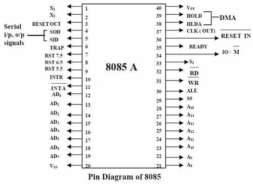
- The 8085 has extensions to support new interrupts, with three maskable interrupts (RST 7.5, RST 6.5 and RST 5.5), one non-maskable interrupt (TRAP), and one externally serviced interrupt (INTR).
- Three control signals are available on chip: (i) RD : it is a active low signal. Which indicate that the selected IO or Memory device is to be read and data is available on the data bus. (ii) WR : it is a active low signal which indicate that the data on the data bus are to be written into a selected memory or IO location. (iii) ALE : it is a +ve going pulse generated every time the 8085 begins an operation (machine cycle), which indicate that the bits on AD7-AD0 are address bits.
- Three status signals are available on chip: (i) IO/M : this is a status signal used to differentiate between IO and Memory operations. If it is high then IO operation and If it is low then Memory operation. (ii) S1 and S0 : status signals similar to IO/M, can identify various operations that are rarely used in the systems.
Internal Architecture of 8085 Microprocessor
The architecture of 8085 consists of three main sections, ALU (Arithmetic and Logical Unit), timing and control unit and Registers (shown in the following figure).
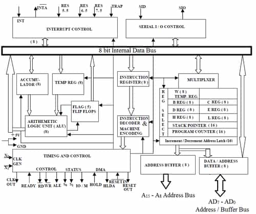
Arithmetic and Logic Unit (ALU): The ALU performs the actual numerical and logical operations.
- The ALU performs the following arithmetic and logical operations.
- Addition, Subtraction
- Logical AND, Logical OR, Logical Ex - OR
- Complement (logical NOT)
- Increment, Decrement
- Left shift, Right shift
- Clear, etc.
- ALU includes the accumulator, the temporary register, the arithmetic and logic circuits and flags. It always stores result of operations in Accumulator.
Timing & Control Unit: It generates timing and control signals, which are necessary for the execution of instructions.
- It controls data flow between CPU and peripherals (including memory).
- It provides status, control and timing signals, which are required for the operation of memory and I/O devices.
- 8085 System Bus: Microprocessor communicates with memory and other devices (input and output) using three buses: Address Bus, Data Bus and Control Bus.
- Address Bus: The Address bus consists of 16 wires. The size of the address bus determines the size of memory, which can be used. To communicate with memory the microprocessor sends an address on the address bus to the memory. Address bus is unidirectional, i.e., numbers only sent from microprocessor to memory.
- Data Bus: Bus is bidirectional. Size of the data bus determines what arithmetic can be done. Data bus also carries instructions from memory to the microprocessor.
- Memory size = 2A x D where, A denotes the address lines, and D denotes the data lines.
- Control Bus: Control bus are various lines which have specific functions for coordinating and controlling μP operations. The control bus carries control signals partly unidirectional, partly bidirectional. Control signals are things like read or write.
Registers: 8085 has six general-purpose registers to store 8 bit data, these are identified as B, C, D, E, H and L . They can be combined as register pairs BC, DE and HL to perform some 16 bit operations.
- Accumulator: The accumulator is an 8 bit register included as a part of Arithmetic Logic Unit (ALU). This register is used to store 8 bit data and to perform arithmetic and logical operations. The result of an operation is stored in the accumulator.
- Flag Register: The ALU includes five flip-flops. They are called Zero (Z), Carry (CY), Sign (S), Parity (P) and Auxiliary Carry (AC) flags. The microprocessor uses these flags to test data conditions. The conditions (set or reset) of the flags are tested through the software instructions. The combination of the flag register and the accumulator is called Program Status Word (PSW) and PSW is the 16-bit unit for stack operation.

- Program Counter (PC): This 16 bit register deals with sequencing the execution of instruction. The microprocessor uses this register to sequence the execution of the instructions. The function of the program counter is to point to the memory address from which the next byte is to be fetched.
- Stack Pointer (SP): The stack pointer is also a 16 bit register used as a memory pointer. It points to a memory location in read-write memory, called the stack.
- Instruction Register/Decoder: Temporary store for the current instructions of a program. Latest instruction sent here from memory prior to execution. Decoder then takes instruction and decodes or interprets the instruction. Decoded instruction then passed to next stage.
- Memory Address Register: Holds address, received from PC of next program instruction.
- Control Generator: It generates signal within μP to carry out the instructions which have been decoded.
- Register Selector: This block controls the use of the register stack.
- General Purpose Registers: μP requires extra registers for versatility. It can be used to store additional data during a program.
Operations of Microprocessor
The microprocessor performs the following four operations using address bus, data bus, and control bus:
- Memory Read: Reads data (or instruction) from memory.
- Memory Write: Writes data (or instruction) into memory.
- I/O Read: Accepts data from input device.
- I/O Write: Sends data to output device.
8051 Microcontroller architecture

pin diagram of 8051

- Pins 1 to 8− These pins are known as Port 1. This port doesn’t serve any other functions. It is internally pulled up, bi-directional I/O port.
- Pin 9− It is a RESET pin, which is used to reset the microcontroller to its initial values.
- Pins 10 to 17− These pins are known as Port 3. This port serves some functions like interrupts, timer input, control signals, serial communication signals RxD and TxD, etc.
- Pins 18 & 19− These pins are used for interfacing an external crystal to get the system clock.
- Pin 20− This pin provides the power supply to the circuit.
- Pins 21 to 28− These pins are known as Port 2. It serves as I/O port. Higher order address bus signals are also multiplexed using this port.
- Pin 29− This is PSEN pin which stands for Program Store Enable. It is used to read a signal from the external program memory.
- Pin 30− This is EA pin which stands for External Access input. It is used to enable/disable the external memory interfacing.
- Pin 31− This is ALE pin which stands for Address Latch Enable. It is used to demultiplex the address-data signal of port.
- Pins 32 to 39− These pins are known as Port 0. It serves as I/O port. Lower order address and data bus signals are multiplexed using this port.
- Pin 40− This pin is used to provide power supply to the circuit.
8051 Interrupts
Interrupts are the events that temporarily suspend the main program, pass the control to the external sources and execute their task. It then passes the control to the main program where it had left off.
8051 has 5 interrupt signals, i.e. INT0, TFO, INT1, TF1, RI/TI. Each interrupt can be enabled or disabled by setting bits of the IE register and the whole interrupt system can be disabled by clearing the EA bit of the same register.
IE (Interrupt Enable) Register
This register is responsible for enabling and disabling the interrupt. EA register is set to one for enabling interrupts and set to 0 for disabling the interrupts. Its bit sequence and their meanings are shown in the following figure.
EA | IE.7 | It disables all interrupts. When EA = 0 no interrupt will be acknowledged and EA = 1 enables the interrupt individually. |
- | IE.6 | Reserved for future use. |
- | IE.5 | Reserved for future use. |
ES | IE.4 | Enables/disables serial port interrupt. |
ET1 | IE.3 | Enables/disables timer1 overflow interrupt. |
EX1 | IE.2 | Enables/disables external interrupt1. |
ET0 | IE.1 | Enables/disables timer0 overflow interrupt. |
EX0 | IE.0 | Enables/disables external interrupt0. |
IP (Interrupt Priority) Register
We can change the priority levels of the interrupts by changing the corresponding bit in the Interrupt Priority (IP) register as shown in the following figure.
- A low priority interrupt can only be interrupted by the high priority interrupt, but not interrupted by another low priority interrupt.
- If two interrupts of different priority levels are received simultaneously, the request of higher priority level is served.
- If the requests of the same priority levels are received simultaneously, then the internal polling sequence determines which request is to be serviced.
- | IP.6 | Reserved for future use. |
- | IP.5 | Reserved for future use. |
PS | IP.4 | It defines the serial port interrupt priority level. |
PT1 | IP.3 | It defines the timer interrupt of 1 priority. |
PX1 | IP.2 | It defines the external interrupt priority level. |
PT0 | IP.1 | It defines the timer0 interrupt priority level. |
PX0 | IP.0 | It defines the external interrupt of 0 priority level. |
8051 Microcontroller Instruction

You can avail of Online Classroom Program for all AE & JE Exams:
Online Classroom Program for AE & JE Exams (12+ Structured LIVE Courses and 160+ Mock Tests)
You can avail of BYJU'S Exam Prep Test Series specially designed for all AE & JE Exams:
BYJU'S Exam Prep Test Series AE & JE (160+ Mock Tests)
Thanks,
Team BYJU'S Exam Prep
Sahi Prep Hai to Life Set Hai !!!
Download BYJU'S Exam Prep APP , for best Exam Preparation , Free Mock Test, Live Classes


Comments
write a comment