Consider the diode circuit shown in the figure below:
If the diode are ideal and the input voltage is a 1 kHz sine wave with a peak voltage of 10V, then the output waveform can be represented as
Question 2
Find the overall transfer function of the control system whose signal flow graph is shown in figure below.
Question 3
In the circuit shown in figure, voltage V0 is
Question 4
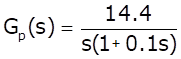
The open loop transfer function of a system with unity negative feedback system is given by
For K=2, the nyquist plot of G(s) encircles the point (-1+j0)
Question 5
For the given circuit determine the coefficient of coupling k, for series resonance condition.
Question 6
Calculate drain current in n channel MOSFET having VT = 0.6 V, w = 35 μm, L = 3 μm, μn = 655 cm2/v-s, Tox = 425 A°, relative permittivity is 3.8, VGS = 2 VT, VDS = VDS (sat).
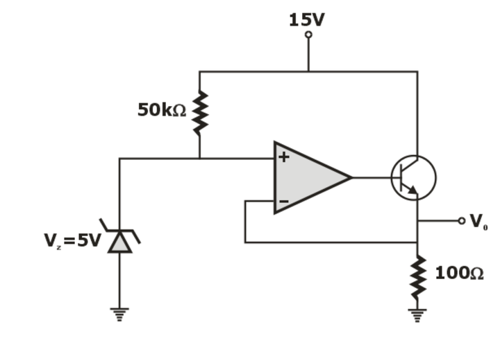
Question 7
If the op-amp in the circuit shown in figure below is ideal then the value of current supplied by the 15 V supply is (Assume β of the transistor to be very large).
Question 8
Find the equivalent resistance across terminals A and B i.e. RAB in ohms?
Question 9
The neutral base width of a bipolar transistor, biased in the active region, is 0.5 μm. the maximum electron concentration and the diffusion constant in the base are 1014/cm3 and Dn = 25 cm2/sec respectively. Assuming negligible recombination I the base, the collector current density is (the electron charge is 1.6 × 10⁻¹⁹ coulomb)
Question 10
Find the ABCD parameter matrix for the given circuit
Question 11
In the voltage doubler circuit shown in the figure, the switch ‘S’ is closed at t = 0. Assuming diodes D1 and D2 to be ideal, load resistance to be infinite and initial capacitor voltages to be zero. The steady state voltage across capacitor C1 and C2 will be
Question 12
In the series voltage regulator circuit shown below VBE = 0.7 V, β = 50, VZ = 8.3 V. The output voltage V0 is _____ volts.
Question 13
The parameters in the base region of an npn bipolar transistor are Dn = 20 cm2/s, nB0 = 104 cm-3, xB = 1 μm, ABE = 10-4 cm2. What will be the collector current (in μA) for VBE = 0.5 V?
Question 14
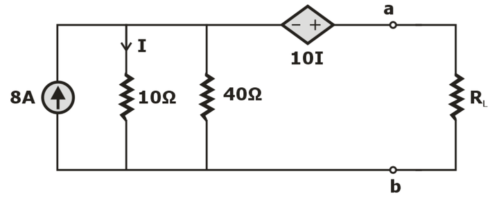
In the circuit shown in figure below, what is the value of RL such that maximum power is transferred to the load?
Question 15
The OP Amp circuit shown in figure is
Question 16
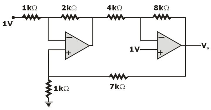
Find the output voltage of the following circuit assume the ideal op-amp behavior.
______ V.
Question 17Multiple Correct Options
Consider a Zener Regulator circuit as shown in the figure below:
The regulator have
(i) Knee current = 5 × 10⁻³ A
(ii) Maximum allowed power dissipation = 300 mW
(iii) Output voltage that is to kept = 6 V
Then which of the following statement is/are correct with respect to zener regulator circuit?
Question 18
Find the current in 4Ω resistor?
Question 19
For the circuit shown in figure below, the value of voltage across capacitor v(t) for t > 0 is
Question 20
A system is shown in below.
If R(s) is unit impulse input, the rise time and settling time for this system is
Question 21
Given astable multivibrator generate sq wave of 10 kHz with 60% duty cycle. It uses a capacitor of 500 pF. Find the value of R1 of R2
Question 22
Consider a closed-loop system as shown. is the plant transfer function and Gc(s) = 1 is the compensator. For a unit-step input, the output response has damped oscillations. The damped natural frequency is ________ rad/s. (Round off to 2 decimal places.)
Question 23
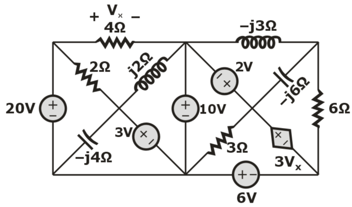
Find the value of current Ix in the following circuit is (in Ampere) ______.
Question 24
The switch S in the circuit of figure has been closed for a long time and is opened at t = 0. The current i(t) for t > 0 is
Question 25
A system has the input-output relation: ,where c (t) is the output to the system. Determine the unit step response of the system.


 is the plant transfer function and Gc(s) = 1 is the compensator. For a unit-step input, the output response has damped oscillations. The damped natural frequency is ________ rad/s. (Round off to 2 decimal places.)


